The Raspberry Pi has 54 GPIO pins (pins 0 to 53) that can be used to interact with external sensors and devices. GPIO pins are peripherals, and they are controlled via special memory locations called peripheral registers. Keep in mind that peripheral registers are not the same as the other registers we learned about (r0–r15).
To control the GPIO pins, we use the four gpio peripheral registers: FSEL, SET, CLR, and LEV. The table below shows
the memory addresses of these registers. (Some of the addresses are labeled "Reserved", which means we don't want to mess with them.)
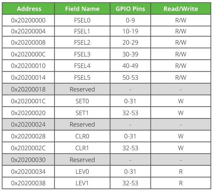
I adapted this table from the Broadcom BCM2835 ARM Peripherals datasheet, p.90!
Notice that there are six FSEL registers but only 2 each of SET, CLR, and LEV. Why is this? Each FSEL register is listed as controlling 10 GPIO pins, such as FSEL0 for pins 0-9. The SET0 register covers 32 pins, from 0 to 31. The SET, CLR, and LEV registers deal with pins being on or off, a state which can be represented with a single bit per pin. In contrast, a FSEL register is used to set the function
of a pin, of which there are eight possible settings (input, output, ALT0-ALT5). To distinguish eight different possibilites requires three bits, so we can fit at most 10 pins (= 30 bits) into a 32-bit FSEL register (with 2 bits left over). Thus to control all 54 GPIO pins requires six FSEL registers and 2 each of SET/CLR/LEV.
Configure a pin:FSEL
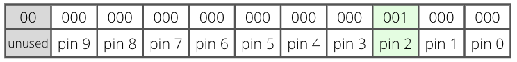
The FSEL registers are used to set the function of a GPIO pin. The eight different pin functions are Input, Output, and six Alternate functions 0-5. Each function is represented as three bits. For example, the Input function is 000 and Output function is 001.
The Output function configures a pin to be used as an output. We can change the value of an output pin using SET and CLR. This lets us turn on LEDs, for example.
The Input function configures a pin to be used as an input. We can read the value of the pin using LEV. This lets us determine whether a button has been pressed, for example.
To set GPIO pin 3 as an output, for instance, we would set bits 6-8 (highlighted below) to 001 in the FSEL0 register.
Turn on a pin: SET
The SET registers are used to turn on a GPIO output pin. (We cannot turn off a GPIO output pin with SET, instead see CLR below).
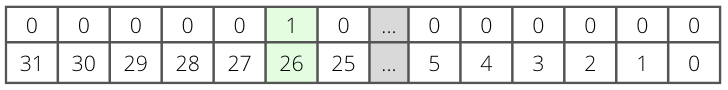
For example, if we wanted to turn on GPIO pin 26, we could write the value 0b00000100000000000000000000000000 into the SET0 register. That will turn on pin 26.
SET registers are write-only. You write to the register to turn a pin on, but it is not possible to read from the reigster to get the current state. (Technically, it will let you read the SET register, but you can't trust that the values will be accurate. Instead see LEV below.)
Turn off a pin: CLR
The CLR registers are used to turn off a GPIO output pin. Writing a 1 to a specific bit in the CLR register will turn off
the pin. It is not intuitive—you would assume that you write a 1 to turn something on, and a 0 to turn something off! to turn off (CLR) is separate from the mechansim to turn on (SET). In both cases, we write a 1, and whether this causes the pin to turn on or off is determined by whether we are writing the 1 into the SET register or the CLR register.
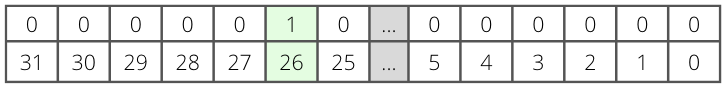
Writing 0b00000100000000000000000000000000 into the CLR0 register would turn off GPIO pin 26. This is the same value used to turn on pin 26, but we write the value to a different address (0x20200028, CLR0, instead of 0x2020001C, SET0).
Like SET, CLR registers are write-only. Reading from the CLR register cannot be used to reliably read the current state.
Read a pin: LEV
The LEV registers are used to read the on-off value of a GPIO pin. The LEV value can be read for any pins, whether it is an input or an output pin. It makes most sense to read the
LEV of an input pin, because we haven't set that value ourselves (it's from an outside source). LEV registers are laid out like SET and CLR registers (32 bits,
representing 32 pins). If the bit value is 1, the corresponding gpio is on, and if 0, it is off.
LEV registers are read-only. We can't write to a LEV register to turn on or off a pin (use SET
or CLR instead).